Ultimate Guide to Benchtop PCB Rework & Repair
The reality is that no soldering operation produces perfect assemblies every time. Even the highest quality components fail from time-to-time. That’s why understanding the best rework and repair methods and materials is so important for those who manufacture, maintain, or fix PCB board issues.
Safe PCB Handling & Static Prevention
The safest way to handle PCBs when repairing them is to wear safety glasses, discharge electronics, prevent static discharge, and reduce contamination.
Care needs to be taken when handling printed circuit boards (PCBs) to prevent causing more damage than you are repairing. These are issues to be concerned about:
- Wear safety glasses: Solder can splatter or leads can fly when trimmed, so wear safety glasses to protect your eyes anytime you are repairing a PCB.
- Unplug and discharge your electronics: To prevent short circuiting the electronics and possibly electrocuting yourself, make sure the device you are repairing is unplugged and fully discharged. Capacitors and power supplies can hold a charge, so pay extra attention to make sure they are fully discharged. If there are any supplemental batteries, disengage those as well.
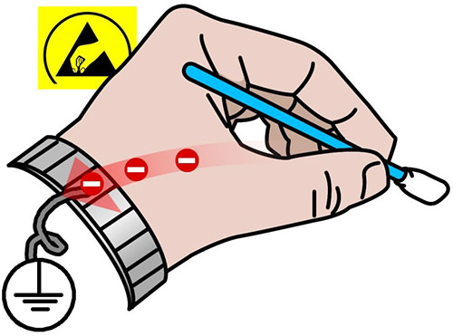
- Prevent static discharge: Electrostatic discharge (ESD) happens all the time, especially in dry climates and in the winter season, when there isn’t moisture in the air to help bleed off excess electrons (water is conductive, so allows the electrons to flow more readily). ESD is the sudden flow of electrons, or spark, from one surface to another. This is caused by a differential between the two surfaces, so one has more electrons than another. Nature loves equilibrium, so the electrons are exchanged to equalize the distribution. Normally it is nothing more than an irritation, but with sensitive electronics, it can lead to PCB failures. Wearing a grounded wrist strap and working on a grounded ESD-safe mat is the best way to prevent ESD. A wrist strap has a conductive surface that touches the skin, so can bleed off excess electrons. Grounded wrist straps bleed off excess electrons to prevent damaging static discharge. An ESD-safe mat works by a similar principle, so bleeds off a charge from anything on its surface. If working on a PC, you can clip the wrist strap directly to an unpainted area of the case.
- Reduce contamination by washing hands and handling only the edges of the PCB: Contamination from your hands can create solderability issues and possibly lead to board failure from corrosion or dendritic growth. Silicone in your hand lotion or picked up from somewhere can create a barrier on contact areas which, in a soldering process, could prevent the solder from creating a good metallurgic bond. The solder may stick temporarily but pop off when exposed to any kind of thermal or physical stress. Contamination, like salt on those fries you had with lunch, are another leading cause of problems introduced in the repair process. Salt is an ionic soil which, when combined with moisture from the air, can cause corrosion. The ionic particles can also join to form dendrites, which can lead to current leakage and even short circuiting. Washing your hands and using only electronic-safe hand lotion is a good way to prevent this type of board failure. Also holding the board only by the edges without contacts (e.g. gold fingers) can help prevent depositing contamination on any critical areas.
Associated products:
Solder Removal & Desoldering Methods
To reduce thermal stress, heat and remove the solder joint and the component as quickly as possible while not heating surrounding areas unnecessarily.
Heating only the solder joints required to remove the defective components and performing the task quickly reduces thermally stressing other areas. Solder wick or desoldering stations are good methods to remove solder from isolated areas. Methods involving hot plates or hot air have a better chance of causing PCB failure later on.
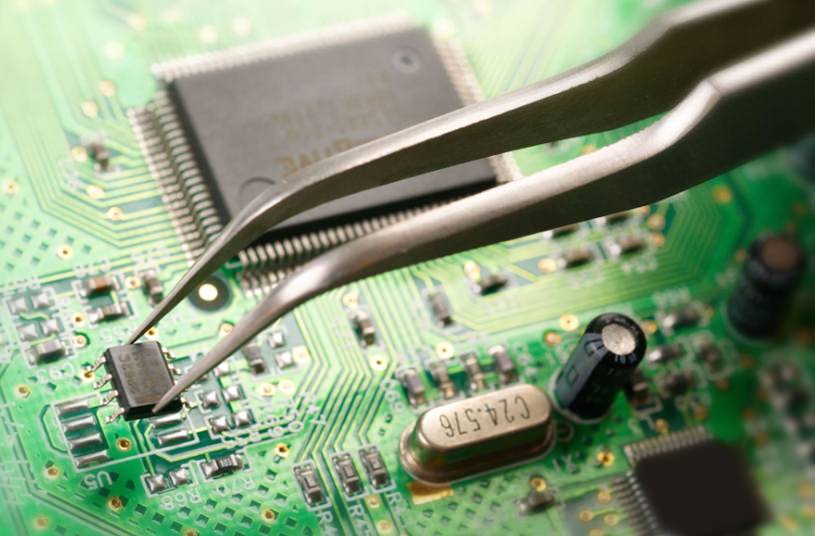
Soldering is a fairly simple concept of combining two metal surfaces using a hot soldering iron, flux, and solder. Removing the same solder if something isn't right is more complicated. Bad components may need to be removed and replaced, or excessive solder may need to be removed, like with bridging between two contacts.
The following are common methods of solder removal, also called "desoldering":
| Method | Description | Considerations |
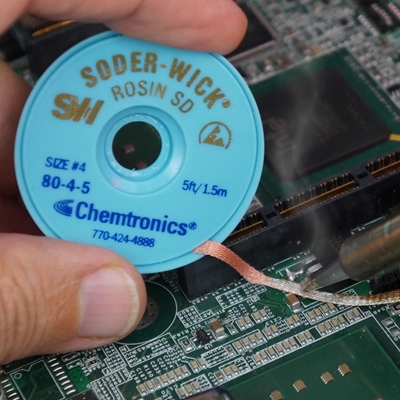
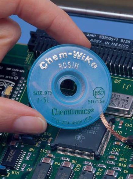
| Solder Wick | Solder wick, desoldering wick, or just "wick" are all names for a copper braid that is used to absorb solder. It is generally coated with flux so that when heated solder is melted, drawn up, and retained using a combination of wetting and capillary action. | Solder wick allows you to remove solder in isolated areas without thermally stressing the overall board or nearby components. Solder wick can only remove exposed solder, so components covering contact areas, like ball grid arrays (BGAs), have to be removed before the residual solder can be removed. |
| Solder Suckers | Solder suckers use a spring-loaded vacuum to draw up melted solder. The solder needs to be melted either with a soldering iron or hot air, like from a heat gun or rework station. | Only small amounts of solder are drawn up at a time, or it often takes multiple attempts to remove a component. Maintaining soldering temperature or remelting a solder joint over-and-over increases the thermal stress on components, other solder joints, and the overall circuit board. Solder suckers can only remove exposed solder. |
| Desoldering Stations | Desoldering stations have a soldering tip with a hole in the middle that draws up the solder once it is melted. | While a very efficient method of desoldering, rework stations can only remove exposed solder. |
| Hot Air Solder Stations | These stations blow hot air over the repair area to melt the solder, and the component is removed either with tweezers or a vacuum lifter. | Once the component is out of the way, the solder will need to be removed another way. |
| Hot Tweezers | If you picture grabbing the lead areas with a tweezer made of two soldering irons, you get the general idea. The idea is to clamp onto the leads on both sides of the component to melt all the solder at once. | This limits the overall thermal stress compared to hot air. Once the component is out of the way, the solder will need to be removed another way. |
| Hot Plate | Placing the PCB on a hot plate melts (or reflows) all the solder joints to allow several components to be removed at the same time. | This method may unnecessarily stress other components and the board as a whole. |
Associated products: Desoldering Wick
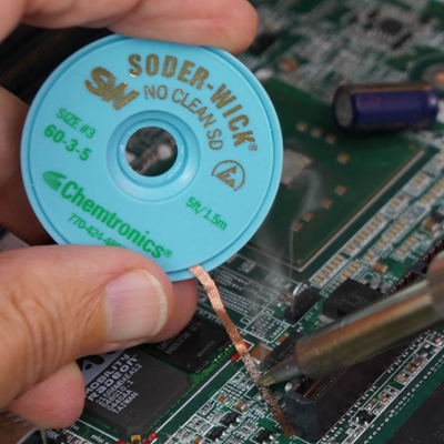
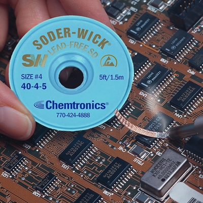
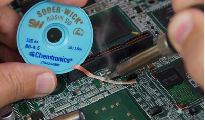
Solder Wick Selection & Proper Usage
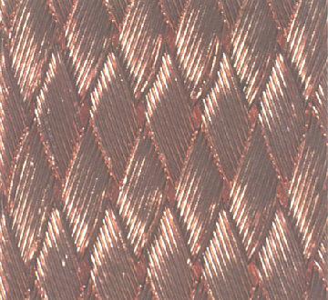
Solder wick, desoldering braid, or just “wick” are all names for a copper braid that is used to absorb solder. It is generally coated with flux so that when heated the solder is melted, drawn up, and retained using a combination of wetting and capillary action. Solder wick allows you to remove solder in isolated areas without thermally stressing the overall board or nearby components. Solder wick can only remove exposed solder, so components covering contact areas, like ball grid arrays (BGAs), have to be removed before the residual solder can be removed.
How to Use Solder Wick:
- Place the braid over unwanted solder, preferably on the greatest solder build up so that it maximizes the contact of the braid to the surface area of the solder.
- Next place your iron tip over the wick at 45 degrees and allow heat to transfer to the pad. Molten solder will absorb into the braid.
- Move the solder tip and braid as needed to remove all of the solder at one time. Be careful not to drag the braid over the pads as it could scratch.
- Once the braid is full of solder, you must trim the spent portion and move to fresh braid in order to pull more solder. Remove the iron and braid simultaneously to avoid soldering the wire to the board.
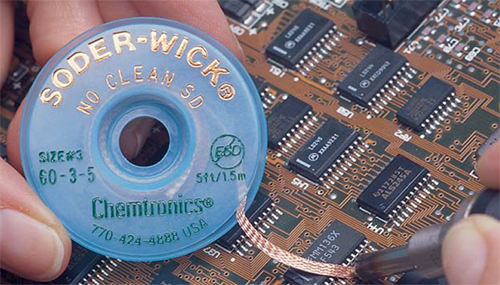
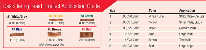
Selecting the Right Solder Wick Size: Solder wick comes in a wide variety of widths to efficiently remove solder from different types of contact areas. Wick that is too thin won't remove enough solder and requires you to trim and remelt the solder over and over. Wick that is too wide takes longer to heat and may interfere with other components on the circuit board. Choose a desoldering wick width that closely matches the size of the contact area. This will ensure that you get proper heat conduction and that you don’t desolder unwanted areas. Widths of desoldering wire are designated by the numbers 1 through 6 or by color codes, and these are standard across the industry:
- #1/white braid is the smallest (under 1mm wide) and is mainly for SMD’s and microcircuits.
- Most will find #2/yellow, #3/green, and #4/blue to be the most common desolder wire.
- #5/brown is ideal for removing large blobs of solder and #6/red is best for desoldering BGA pads or terminals.
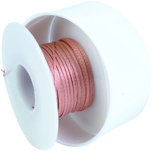
Keep three or four different widths at your work area to cover all cases. Wick can be folded or trimmed at an angle to better fit the contact area. Solder wick can also be packaged in a variety of lengths. 5’ and 10’ lengths are handy for use at a work station. Static dissipative spools, also called “bobbins”, are available to prevent damaging components sensitive to ESD. Longer spools, like 25’ (7.6M), 50’ (15.2M), 100’ (30.5M) and 500’ (152.4M), are commonly stored in a more central location and dispensed to technicians as needed. Other specialized braid designs are also available. For example, Chemtronics offers Solder-Wick Lead-Free, which is engineered to heat faster, so minimizes thermal shock for high-heat lead-free applications.
Common Types of Flux Coating on Solder Wick:
- Rosin: Rosin-fluxed desoldering wick has the fastest wicking action but does leave behind residues that need to be thoroughly cleaned.
- No-Clean: No-clean fluxed desoldering wick is ideal when cleaning isn’t practical or possible. After desoldering, the only thing that remains is a clear, non-ionic residue. For field work, when a thorough cleaning is more challenging, this is the type of braid to use.
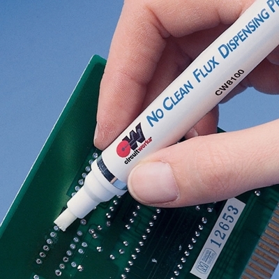
- Unfluxed: In a production or repair environment where the flux is specified and can’t be changed, or when an aqueous flux is needed, you can add your own flux to this type of braid. Unfluxed wick will not remove solder unless flux is added. Different types of fluxes are available in pen packaging, which is ideal for fluxing braid.
Chemtronics offers the following flux pens:
- No-Clean Flux Pens: This no-clean flux is formulated to perform at the elevated temperatures of lead-free soldering but is also effective for tin-lead soldering as well. It's designed with a low surface tension to prevent bridging. Post-soldering cleaning is optional because the light residue left after soldering is barely noticeable is non-corrosive and halide free. This is a good choice for tin-lead soldering where cleaning is to be avoided.
- Rosin Flux Pen: This is a high solid type R rosin flux which provides excellent solderability in a wide variety of applications. The residue left behind is non-corrosive and is halide-free, but it is best to remove the residue after soldering for aesthetics.
- Water Soluble Flux Pen: This is a very active pH neutral ORH1 flux. It enables easy soldering of both lead-free and lead-containing solders. This flux must be cleaned and can be removed easily with DI water, like in a batch or in-line system, or benchtop cleaning with Flux-Off® Water Soluble Flux Remover.
Associated products:
6 Tips for Efficient, High Quality Desoldering
- Keep Your Soldering Iron Tip Clean and Tinned For Effective Heat Conduction: This might seem like a no-brainer, but it’s often overlooked and critical for efficient desoldering. Soldering iron tips covered with burnt flux and oxidation will not wet (accept solder) and will conduct heat poorly. A clean and tinned soldering tip conducts heat through the desoldering braid better and starts the wicking action faster.
- Minimize the Length of Time That the Board and Components Remain at a High Temperature: Applying high heat levels to the board or its components for an extended period of time can damage your board, components, create brittle solder joints, and lead to service issues down the round.
- Match Wick Width to Solder Joint or Contact Pad: Desoldering wick generally comes in several different widths so you can match the braid to what you are desoldering. Wick that is too thin won't remove enough solder and requires you to trim and remelt the solder over and over. Wick that too wide takes longer to heat and may interfere with other components on the circuit board.
- Match Soldering Iron Tip to Braid Width for Accuracy: Use a soldering tip that is roughly the width of the braid and contact area. A tip that is too small will require more dwell time. A tip that is too large runs the risk exposing other components in a dense assembly. Matching the tip size allows you to melt the unwanted solder faster and minimizes the time that heat is applied. Use a blade or knife tip when desoldering large areas, like a BGA pad.
- Match Flux Type to Your Cleaning Process: Desoldering braid is available in various flux types depending on your cleaning process and other requirements. Rosin fluxed braid has the fastest wicking action but leaves behind residues that need to be thoroughly cleaned. No-clean fluxed braid is ideal when cleaning isn’t practical or possible. After desoldering the only thing that remains is a clear, non-ionic residue. For field work, when thorough cleaning is more challenging, this is the type of braid to use.
- Protect Your Board Against Corrosion By Using a Quality Flux Remover: Flux residues can cause dendritic growth and corrosion on PCB assemblies, so make sure you’re using best practices and clean the board. After all the components have been replaced and excess solder removed clean the area thoroughly with a quality flux remover.
Associated products: Desoldering Wick
Removing Excess Solder from BGA Pads
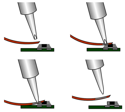
Large amounts of solder on large pads or ball grid arrays (BGAs) can be removed using a solder sucker and hot air, but that requires exposing the PCB to high temperatures for an extended period of time, which can thermally stress other components and the board as a whole. Solder wick is a faster and less thermally stressful method of removing solder from a large area. Solder wick is available in wider configurations, from 3 to over 5mm. 3.5 to 4mm width is identified as #5 or brown wick, and 5 to 5.5mm as #6 or red wick. The soldering tip geometry should be matched as closely as possible to the width of the braid. Tips with a large flat surface, such as a screwdriver, chisel, bevel, or knife shape, tend to work best. Many technicians make the mistake of holding the soldering tip on the surface of the braid and then dragging the braid across the pads to remove the molten solder. The dragging motion can scratch the surface of the pads or the OSP coating.
The following is the best-practices technique that we recommend:
- Apply the braid over the pads to be desoldered.
- Apply the hot soldering tip on one end of the braid.
- Holding the braid still, drag the soldering tip up the braid. There is no need to apply pressure on the iron. That only risks pulling the braid and scratching pads. The weight of the soldering iron should be enough to do the job.
- Lift the braid while it is still hot and repeat the above steps on the next row of pads. Make sure to trim off spent braid before moving to this step. Excess braid acts as a heat sink, so it will take longer to heat up.
Associated products: Desoldering Wick
Cleaning PCBs & Removing Solder Flux
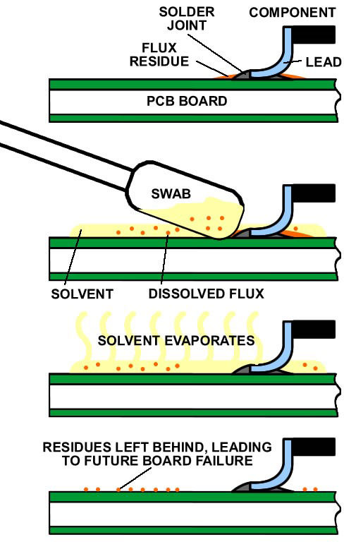
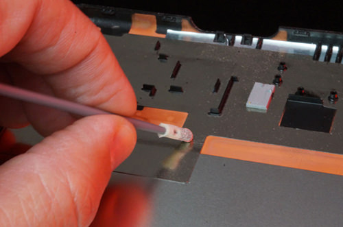
The most common way to clean flux residues from a repair area is to saturate a cotton or foam swab with isopropyl alcohol or another cleaning solvent and rub it around the repair area.
While this may be adequate for no-clean flux, where the goal is a visually clean PCB, this may not be clean enough when more heavily activated fluxes are involved, like RA or aqueous. The dirty little secret is that flux residues will not evaporate along with the solvent. You may dissolve the flux, and some of the residues will soak into the swab, but most of the residues will settle back onto the board surface. Many times these white residues are more difficult to remove than the original flux.
One quick and easy improvement to this process is to rinse the board after swabbing around the repair area. While the solvent is still wet, spray over the entire board with an aerosol flux cleaner. Hold the PCB at an angle to allow the solvent to flow over the board and run off along with any residues that are picked up. The straw attachment that comes with aerosol flux removers is a good way to increase the spray force and penetrate beneath components.
Chemtronics offers the BrushClean system with many of their flux removers. The cleaning solvent sprays through the brush, so agitation can be increased by scrubbing while spraying. To absorb the flux residues, a lint-free poly-cellulose wiper can be placed over the repair area, and the spraying and scrubbing can occur over the material. Then remove the wipe and brush attachment, and spray over the board for the final rinse.
Associated products:
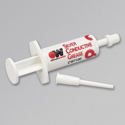
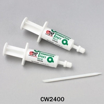
Connecting Temperature-Sensitive Components
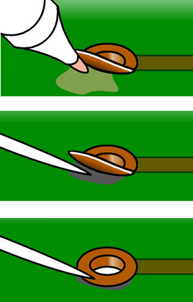
Two-part conductive epoxy is a great solution for making solderless electronic connections. This type of epoxy contains conductive material so, when cured, it forms a very strong and highly conductive bond similar to a solder joint. Chemtronics offers two options: CircuitWorks® Conductive Epoxy, which cures in 10 minutes, and CircuitWorks® 60 Minute Conductive Epoxy, which provides more time to work. Both Epoxies have A and B components that need to be thoroughly mixed before the curing process will begin. Once mixed, you use the included plastic pick to apply epoxy to the connection. If movement may occur during the curing process, you will need to tape down or otherwise secure the wires or components.
Associated products: CircuitWorks Conductive Epoxy
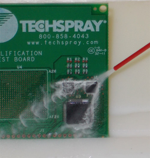
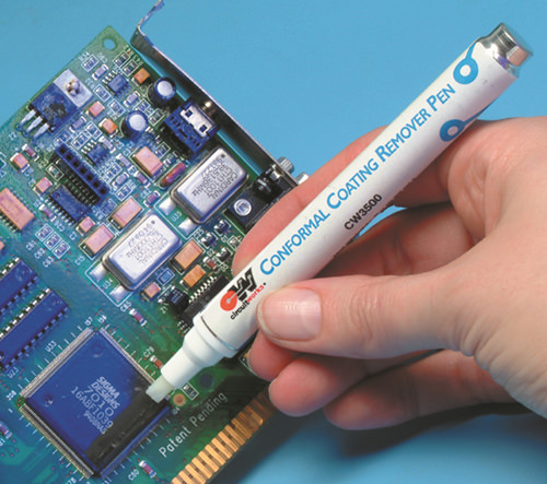
Removing & Patching Conformal Coating
The best method of removing a coating depends on the type of coating and the sensitivity of the components:
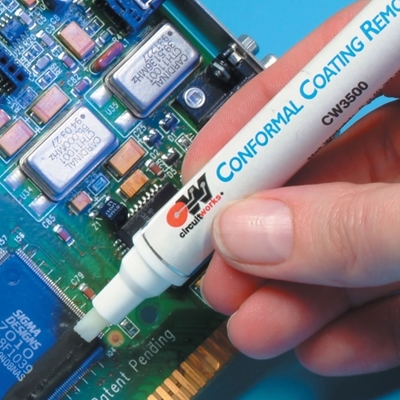
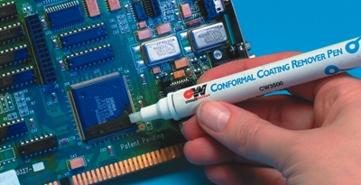
- Acrylic (AR) / Silicone (SR) / Urethane Coatings (UR): When desoldering, it is possible to burn through Acrylic, Silicone or Urethane coatings. This could leave burned or rough edges that will need to be cleaned up before recoating. These coatings can be removed chemically, using either specialized solvents or common solvents, like acetone, toluene, and xylene. All of these are very harsh (which is why they dissolve coatings so well), and toluene and xylene have toxicity issues, so make sure to wear appropriate PPE and have adequate ventilation. Chemtronics offers the CircuitWorks® Conformal Coating Remover Pen that allows you to remove a precise coating piece without affecting the rest of the PCB. You first saturate the tip by tapping it lightly on a surface, which opens the valve and releases solvent. Don’t hold it down as it may oversaturate it, which could lead to solvent flowing into unintended areas. You then rub the pen tip over the coating that you want to remove. You may need to periodically wipe the pen tip on a wiper to remove accumulated resin. The tip will continue to resaturate as you apply pressure as you clean. Don’t press hard as it could lead to excessive solvent flowing over the board. Let the solvent do the work, and give it the time necessary to break down the coating resin. Acrylic coating will break down quickly, but silicone and especially urethane will take more time.
- Epoxy Resin (ER) / Parylene (XY): Epoxy and parylene coatings are incredibly tough coatings, and resistant to physical and chemical stresses. Of course, the properties that make them so effective also make them difficult to remove. You can’t strip these resins using a chemical. Burning or melting them off may be possible, but risks damaging the PCB as well. The micro-abrasive blasting method is generally the accepted way of removing epoxy and parylene coatings. Micro-abrasive blasting uses a specialized device to blow abrasive particles over the coated surface. The abrasive medium needs to be chosen with great care so the process doesn’t damage the remaining surface, components or markings. The area around the repair should be masked to isolate the effect of the blasting.
- Ultra-Thin Coating (UT): Ultra-thin coating, which is becoming more common for consumer electronics like mobile phones, should not have to be removed. It is invisible to the naked eye, and easily burns and scrapes away.
Associated products: CircuitWorks Conformal Coating Remover Pen
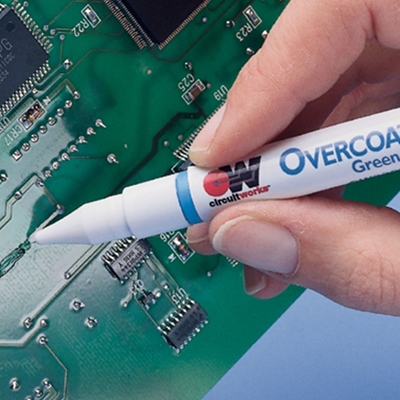
How to Patch the Conformal Coating Ideally, you should use the same coating material as the original PCB assembly, which should be specified in the service manual of the device. In the real world of electronic repair, you may have no idea what was originally applied. In that case, the easiest solution is to coat using an acrylic coating. Chemtronics offers CircuitWorks® Overcoat Pens in a variety of colors to match the PCB resist. Overcoat pens are basically acrylic conformal coating in convenient packaging, and the clear version can be used to coat small areas. Simply press down the pen tip and squeeze the barrel to dispense the coating material. For larger areas, conformal coating can be applied using a small acid brush. No matter how you coat, make sure you avoid coating connectors. Coat around them, or mask them with Kapton tape or temporary solder mask.
Associated products:
Repairing Traces, Pads, Cracks & Shielding
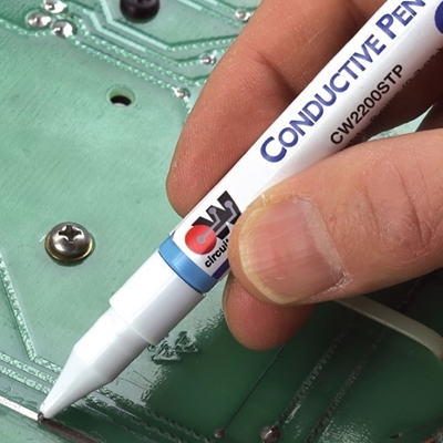
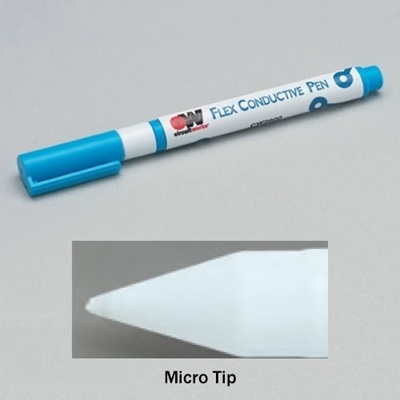
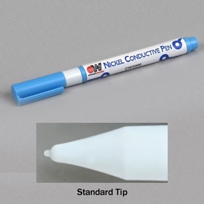
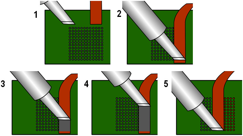
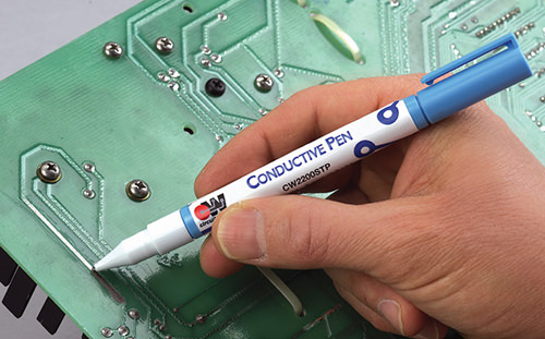
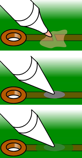
Repairing a Broken Trace A common method of repairing a broken trace is to solder on a jumper, which is basically a wire bypass around the broken trace. This can be time-consuming and visually unappealing. Chemtronics offers CircuitWorks® Conductive Pens which contain a highly conductive material like silver or nickel suspended in a liquid polymer. These pens allow you to literally redraw the trace.
These are the steps to quickly and effectively repair a trace with a conductive pen:
- For good electrical continuity, you need some surface area of the original trace exposed. If there is solder resist right up to the break, use a sharp blade to scrape away about a 1/16” portion of the resist.
- Clean the area with either a swab saturated with a solvent cleaner like isopropyl alcohol (IPA) or a CircuitWorks® Flux Remover Pen.
- Vigorously shake the conductive pen until you hear the internal ball rattle.
- Press the pen tip at the break area and squeeze the pen barrel to dispense the conductive ink.
- Allow the conductive ink at least one hour to cure before repairing the overcoat.
- Use a CircuitWorks Overcoat Pen to repair the resist area in the break area. Overcoat pens come in a variety of colors to match the color of the PCB. Press down the pen tip and squeeze the barrel to dispense the overcoat material.
Associated products:
- CircuitWorks Conductive Pens
- CircuitWorks Conductive Paint
- CircuitWorks Flux Remover Pens
- CircuitWorks Overcoat Pens
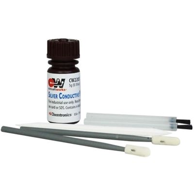
Repairing EMI or RF Shielding Breaks CircuitWorks Conductive Paint is a single component, silver-filled polymer that dries in minutes at room temperature, making it an ideal solution for patching EMI/RFI shielding. The kit comes with brushes, swabs, and a plastic pick to repair large and small areas. In the case of metal screen and wire mesh, it is important that the holes in the screen or mesh are significantly smaller than the wavelength of the electromagnetic radiation being kept out. The goal of such mesh designs is to maintain a consistent hole pattern with a conductive material to ensure electrical continuity. Such a mesh can be repaired by restoring the hole pattern using polyimide tape and CircuitWorks Conductive Paint. Simply apply the polyimide tape to the inside of the mesh and carefully restore the mesh pattern with the CW2205. It is important to ensure that the contact is maintained between the mesh and the conductive paint. A second layer of polyimide tape can be applied to the opposite side for increased durability. Since the polyimide tape is invisible to electromagnetic fields at these wavelengths, the polyimide tape can remain and the EMI shield is restored.
Another common situation is that the aluminum foil inside the shielded cable is damaged. Similar to the case above, this will cause a loss of continuity and could again allow electromagnetic interference. A simple repair in this case is to repair the hole or tear with polyimide tape and then use the CircuitWorks Conductive Paint to paint the tape and restore continuity.
Associated products: CircuitWorks Conductive Paint
Repairing a Damaged Pad on a PCB Standard two-part epoxy can contaminate the surface of the connector, creating an insulative barrier. Two-part conductive epoxy is a great solution for repairing damaged pads. This type of epoxy contains conductive material, so when cured, it forms a very strong and highly conductive bond, like a solder joint. Chemtronics offers two options: CircuitWorks® Conductive Epoxy, which cures in 10 minutes, and CircuitWorks® 60 Minute Conductive Epoxy, which provides more time to work. Both Epoxies have A and B components that need to be thoroughly mixed before the curing process will begin. Once mixed, you use the included plastic pick to apply the epoxy to the connection.
To repair a lifted pad:
- Clean the area with either a swab saturated with a solvent cleaner like isopropyl alcohol (IPA) or a CircuitWorks Flux Remover Pen.
- Apply the mixed conductive epoxy under the pad with the supplied plastic pick.
- Press down the pad.
- Allow the epoxy to fully cure before soldering to the pad.
To replace a damaged pad:
- Cut away the damaged pad.
- For good electrical continuity, you need some surface area of the original trace exposed. If there is solder resist right up to the break, use a sharp blade to scrape away about a 1/16” portion of the resist.
- Clean the area with either a swab saturated with a solvent cleaner like isopropyl alcohol (IPA) or a CircuitWorks Flux Remover Pen.
- Apply the mixed conductive epoxy under the pad with the supplied plastic pick.
- Press down the pad.
- Apply additional epoxy between the pad replacement and the exposed trace.
- Allow the epoxy to fully cure before soldering to the pad.
To repair without a pad replacement:
- Cut away the damaged pad.
- For good electrical continuity, you need some surface area of the original trace exposed. If there is solder resist right up to the break, use a sharp blade to scrape away about a 1/16” portion of the resist.
- Clean the area with either a swab saturated with a solvent cleaner like isopropyl alcohol (IPA) or a CircuitWorks Flux Remover Pen.
- Apply the mixed conductive epoxy over the pad-less area with the supplied plastic pick.
- Place the component lead into the epoxy. For a thru-hole lead, it can be formed into a make-shift gull-wing or J-lead to provide more surface area for the epoxy to grip. Additional epoxy can be applied over the lead for extra security.
- Allow the epoxy to fully cure before handling the PCB.
Associated products: CircuitWorks Flux Remover Pens
Repairing a PCB Crack or Open Area of the Solder Resist This answer assumes the crack does not impact surface or inner-layer traces. CircuitWorks Overcoat Epoxy provides a rugged repair that can in fact reinforce PCB areas with more structural cracks. To use:
- Clean the area with either a swab saturated with a solvent cleaner like isopropyl alcohol (IPA) or a CircuitWorks Flux Remover Pen.
- Mix equal amounts (1:1) by volume of Part A and Part B. Mix thoroughly for one minute.
- Use a brush or pick to apply the epoxy. Pot life is 15-20 minutes at room temperature.
- Tack free time is after 30 minutes at room temperature. Excellent results have been obtained by curing for 10 minutes @ 100°C. Optimum cure cycles using radiant or convection conveyer ovens are best determined experimentally. Product may also be cured for 24 hours @77°F (25°C).
- Clean-Up/Removal (uncured): Use isopropanol, acetate, or MEK to clean-up uncured resin. Cured Epoxy Overcoat cannot be removed using solvents.
Associated products:
Selecting Flux for Component Replacement
Flux is needed to prevent oxidation that tends to form when hot metals encounter air. During printed circuit board repair and soldering, it's common to see liquid flux from the wave soldering equipment poured into jars and applied with an acid brush. That can lead to applying too much flux, forcing an additional cleaning step that might not otherwise be necessary. Other types of flux and special packaging are available that are better suited for PCB repair:
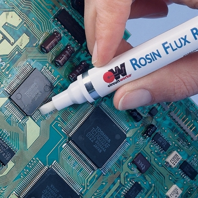
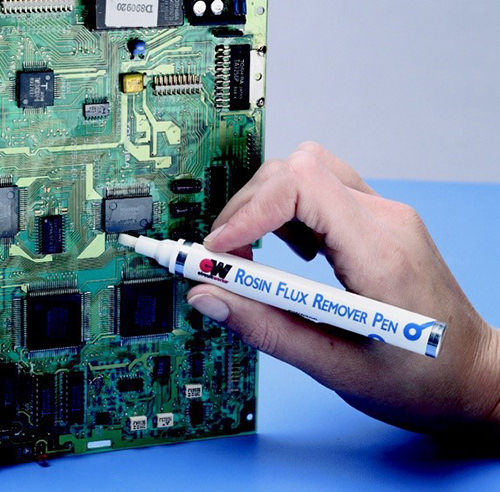
- Flux Pen: Flux pens are valved, prefilled pens of flux. Flux pens avoid the mess and hassle involved in filling your own flux bottles. A flux dispensing pen contains the flux in the airtight barrel of the pen. They are an excellent way to dispense flux for benchtop soldering. You just hold the pen vertically and briefly depress the tip to start the liquid flow. This will saturate the tip of the pen with flux, then you draw flux on the area to be soldered. Gently press the tip again to keep the tip damp with flux. CircuitWorks® flux pens are available with a variety of fluxes to fit your specific shop requirements including: no-clean, high temperature no-clean for lead-free soldering, rosin, and water soluble.
- Tacky Flux: Tacky flux is a viscous, pasty form of flux that is easy to place without it spreading into surrounding areas the way a liquid flux can. It can be used to hold small parts in place before soldering and is common in the manufacture and repair of SMT components. Tacky fluxes in syringe dispensers provide for dispensing convenience similar to a pen but when tacky flux is more appropriate. The thick, honey-like consistency is ideal for ball-attach applications, BGA re-balling and hand soldering SMT components. The flux is dispensed from a syringe and can be spread over the desired area for soldering. CircuitWorks® No-Clean Tacky Flux is a mildly activated rosin (RMA) no-clean tacky flux. Its formulation includes a unique rosin/resin-blend coupled with a proprietary blend of activators and stabilizers providing both significantly increased shelf life and long-term product stability. The remaining residue is stable and can be left on a board without cleaning, or can be easily removed with Flux-Off® No-Clean Plus Flux Remover. CircuitWorks® Lead-Free Tacky Flux is formulated for higher temperatures common in lead-free soldering.
Associated products: CircuitWorks Flux Pens
Repairing Cold Solder Joints
A "cold" solder joint is generally grainy, which is a sign that the solder didn’t melt and wet properly, so you may not have a good metallurgic bond. The connection will most likely break loose with any amount of physical or thermal stress. Be warned that graininess is a visual cue for only lead-based solders. Lead-free solders often look grainy even when there is a good metallurgic bond.
The quickest way to fix a cold solder joint is to simply use a solder iron to remelt the solder. The flux will have been fully activated in the original soldering process, so additional flux can be added using a CircuitWorks® Flux Pen.
- Lightly press the Flux Pen tip to the solder joint until the tip saturates and the flux flows.
- Rub saturated Flux Pen tip over the solder joint.
- Apply the heated solder tip to the solder joint to remelt it.
- If necessary, clean flux residues with either a swab saturated with a solvent cleaner like isopropyl alcohol (IPA) or a CircuitWorks Flux Remover Pen.
Associated products: CircuitWorks Flux Pens
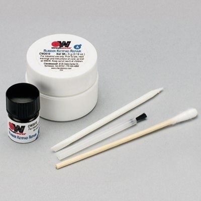
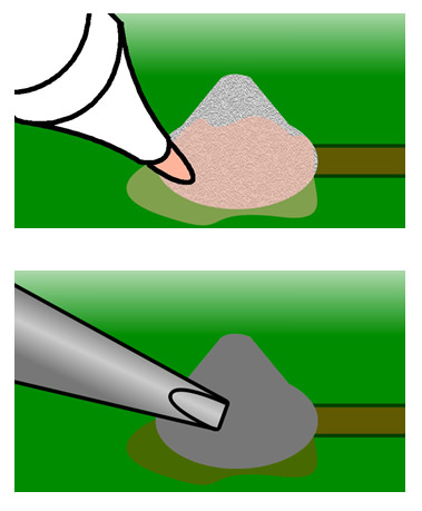
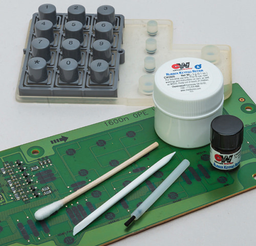
Repairing Black Carbon Conductor Button Pads
Chemtronics offers the CircuitWorks® Rubber Keypad Repair Kit, which can be used to repair keypads by restoring conductivity to worn, intermittent, and nonconductive carbon contacts. It is a two-part mix, and comes with a swab, brush, and plastic pick to help with mixing and applying the materials.
To fix black carbon conductor button pads:
- Clean the area with either a swab saturated with a solvent cleaner like isopropyl alcohol (IPA) or a CircuitWorks Flux Remover Pen.
- Pour the liquid in Part B into the container of Part A. Stir thoroughly for two minutes.
- Paint the worn carbon contacts with the mixed conductive material using the enclosed applicator brushes. Use the least amount of conductive material as possible.
- At room temperature (<75°F / 25°C), the material dries tack-free in one hour. Repaired keypads can be returned to service in 24 hours. Ultimate properties are achieved in 72 hours. For faster drying, expose the material to approximately 190°F (90°C) for 10 minutes. Do not exceed 212°F (100°C).
Associated products:
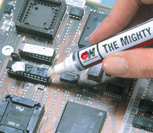
Removing Labels and Sticky Residues
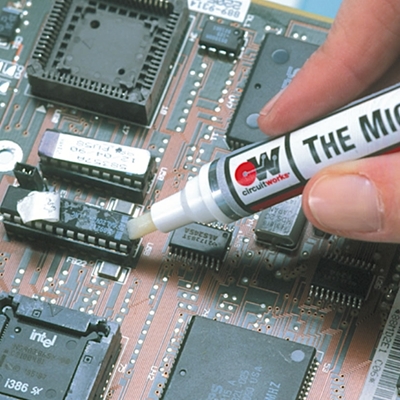
Old identification or QC fault labels can be difficult to remove. They either leave sticky adhesive behind that is insoluble by commonly available solvents like isopropyl alcohol (IPA), or are so dried and baked-on that they won’t budge. While consumer products like Goo Gone or bug-and-tar remover are common to see on workbenches, Chemtronics offers a cleaner that is actually intended for PCB repair called The Mighty Pen®. It contains a fast acting solvent that breaks down dried and sticky adhesives.
How to use The Mighty Pen to remove labels:
- If the label is plastic or covered by a film laminate, you may have to peel it up to allow solvent to penetrate underneath.
- Lightly press the pen tip on the label until the tip saturates enough for solvent to start to flow.
- Rub saturated pen tip over the label area and allow it to soak through.
- Allow the saturated label to sit for at least 15-20 seconds, then rub the area with pen tip until the label material and adhesive are removed.
- Wipe area with clean wiper to remove adhesive residue and solvent.
- Reapply solvent as necessary or allow more soak time for stubborn adhesives.
- If there is adhesive build-up on pen tip, wipe it with a clean wiper.
Associated products: CircuitWorks The Mighty Pen
Frequently Asked Questions (FAQs)
Q: What is the safest way to handle PCBs when repairing them?
A: The safest way to handle PCBs involves wearing safety glasses, ensuring devices are unplugged and discharged, preventing electrostatic discharge (ESD) with a grounded wrist strap and mat, and reducing contamination by washing hands and handling only the edges of the PCB.
Q: Should I be worried about static electricity with handling PCBs?
A: Yes. A typical technician working on a PCB can generate thousands of volts. SMOS logic devices can be damaged with 250-3000 volts, EPROM devices down to 100 volts, and microprocessor chips as low as 10 volts.
Q: Can I add my own flux to solder wick?
A: Yes, unfluxed wick will not remove solder unless flux is added. Different types of fluxes are available in pen packaging, which is ideal for fluxing braid.
Q: How do you clean PCBs after soldering?
A: Saturate a cotton or foam swab with isopropyl alcohol or another cleaning solvent and rub it around the repair area. While the solvent is still wet, spray over the entire board with an aerosol flux cleaner. Hold the PCB at an angle to allow the solvent to flow over the board and run off along with any residues that are picked up.
Q: How do you connect a temperature-sensitive component without high temperature soldering?
A: Two-part conductive epoxy is a great solution for making solderless electronic connections. This type of epoxy contains conductive material so, when cured, it forms a very strong and highly conductive bond similar to a solder joint.
Q: What flux should I use when replacing PCB components?
A: Other types of flux and special packaging are available that are better suited for PCB repair than liquid wave soldering flux. A flux dispensing pen contains the flux in the airtight barrel of the pen and avoids the mess and hassle involved in filling your own flux bottles. Tacky flux is another option; it is a viscous, pasty form of flux that is easy to place without it spreading into surrounding areas the way a liquid flux can.
Q: Is there a quick fix for cold solder joints?
A: A "cold" solder joint is generally grainy, which is a sign that the solder didn’t melt and wet properly, so you may not have a good metallurgic bond. The quickest way to fix a cold solder joint is to simply use a solder iron to remelt the solder.
Q: Is there a good way to remove labels and sticky residues?
A: While consumer products like Goo Gone or bug-and-tar remover are common to see on workbenches, Chemtronics offers a cleaner that is actually intended for PCB repair called The Mighty Pen®. It contains a fast acting solvent that breaks down dried and sticky adhesives.
Ask A Technical Question
Stay up-to-date on Chemtronics news, products, videos & more.
Related Products